Engineers at the University of California, Berkeley (UC Berkeley), have developed an electronic skin, or e-skin, from pressure-sensitive electronic material from semiconductor nanowires, which could someday restore the sense of touch to people using prosthetic devices. They say it is the first such material made out of inorganic single crystalline semiconductors. The research was published in the advanced online edition of the journal Nature Materials on July 21.

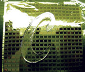
The e-skin was able to accurately sense the shape of the letter placed on top. Photograph courtesy of UC Berkeley.
Previous attempts to develop an artificial skin relied upon organic materials because they are flexible and easier to process. “The problem is that organic materials are poor semiconductors, which means electronic devices made out of them would often require high voltages to operate the circuitry,” said Ali Javey, PhD, an associate professor of electrical engineering and computer sciences at UC Berkeley and head of the research team developing the e-skin. “Inorganic materials, such as crystalline silicon, on the other hand, have excellent electrical properties and can operate on low power. They are also more chemically stable. But historically, they have been inflexible and easy to crack. In this regard, works by various groups, including ours, have recently shown that miniaturized strips or wires of inorganics can be made highly flexible-ideal for high performance, mechanically bendable electronics and sensors.”
The UC Berkeley engineers used an innovative fabrication technique that works somewhat like a lint roller in reverse. Instead of picking up fibers, nanowire “hairs” are deposited. In this case, they were deposited on a sticky polyimide film substrate that formed the basis from which thin, flexible sheets of electronic materials could be built. The engineers then printed the nanowires onto an 18-by-19-pixel square matrix measuring seven centimeters on each side. Each pixel contained a transistor made up of hundreds of semiconductor nanowires. Nanowire transistors were then integrated with a pressure sensitive rubber on top to provide the sensing functionality. The matrix required less than five volts of power to operate and maintained its robustness after being subjected to more than 2,000 bending cycles.
The e-skin-made up of the three distinct electronic components, the thin-film transistor, pressure sensor, and built-in organic light-emitting diodes (OLEDs)-spatially maps the applied pressure but also provides an instantaneous visual response through the OLED display with red, green, and blue pixels. The OLEDs are turned on locally where the surface is touched, and the intensity of the emitted light measures the scale of the applied pressure. The researchers demonstrated the ability of the e-skin to detect pressure from zero to 15 kilopascals, a range comparable to the force used for such daily activities as typing on a keyboard or holding an object.
“This is the first truly macroscale integration of ordered nanowire materials for a functional system-in this case, an electronic skin,” said lead author Kuniharu Takei, PhD, a postdoctoral fellow in electrical engineering and computer sciences. “It’s a technique that can be potentially scaled up. The limit now to the size of the e-skin we developed is the size of the processing tools we are using.”
In addition to providing sensory perceptions to prosthetic limbs, the researchers said the e-skin would help overcome a key challenge in robotics: adapting the amount of forced needed to hold and manipulate a wide range of objects.
Editor’s note: This story was adapted from materials provided by UC Berkeley.


