Researchers at Sandia National Laboratories (Sandia), Albuquerque, New Mexico, are using off-the-shelf equipment in a chemistry lab to work on ways to improve neuroprosthetic device interfaces.

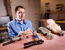
Buerger displays implantable and wearable neural-interface electronics developed by Sandia as he sits in the prosthetics lab with a display of prosthetic components. Photograph by Randy Montoya, courtesy of Sandia National Laboratories.
Organic materials chemist Shawn Dirk, robotics engineer Steve Buerger, and others are creating biocompatible interface scaffolds. The goal is improved prostheses with flexible nerve-to-nerve or nerve-to-muscle interfaces through which transected nerves can grow, putting small groups of nerve fibers in close contact to electrode sites connected to separate, implanted electronics. Researchers are looking at flexible, conducting electrode materials using thin, evaporated metal or patterned, multi-walled carbon nanotubes. The work is in its early stages.
“If we can get the right material properties, we could create a healthy, long-lasting interface that will allow an amputee to control a robotic limb using their own nervous system for years, or even decades, without repeat surgeries,” Buerger said.
Collaborating with the University of New Mexico, Albuquerque Center for Biomedical Engineering and Department of Chemical Engineering, Sandia researchers electrospun scaffolds with two different polymers that are liquid at room temperature-poly(butylene fumarate) (PBF) and poly(dimethylsiloxane) (PDMS). Surgeons at MD Anderson Cancer Center (MD Anderson), Houston, Texas, sutured the scaffolds into legs of rats between a transected peroneal nerve. After three to four weeks, the interfaces were evaluated; however, neither of the interface materials were porous enough.
The team’s search for a different technique to create the porous substrates led to Projection Micro-Stereolithography (PμSL), a process that is capable of fabricating complex 3D microstructures in a bottom-up, layer-by-layer fashion. It couples a computer with a PowerPoint image to a projector whose lens is focused on a mirror that reflects into a beaker containing a solution. Using a laptop and a projector, Dirk said the researchers initially tried using a mirror and a 3X magnifying glass, but abandoned that because it produced too much distortion. They now use the magnifying glass to focus ultraviolet (UV) light onto the PDMS-coated silicon wafer to form thin, porous membranes.
While the lithography technique is not new, “we developed new materials that can be used as biocompatible photo cross-linkable polymers,” Dirk said. The technique allowed the team to create a regular array of holes and to pattern holes as small as 79 microns. Now researchers are using other equipment to create more controlled features.
“It’s exciting because we’re getting the feature size down close to what is needed,” Buerger said.


